|
Diodes and transistors are electronic devices built by combining n-type and p-type semiconductors. Consider what happens at a p-n junction where p-type and n-type semiconductors meet. Initially the n side has free electrons and the p side has holes. Negative electrons from the n side flow over to the p side and combine with positive holes. The n side becomes positively charged and the p side becomes negatively charged. In silicon, electrons move until the charge difference is 0.6 V, enough to keep any additional electrons from crossing over. 
|

|
Right at the p-n junction itself, a depletion region forms that has neither electrons nor holes. The depletion region is an insulator because it has no movable charges that can carry current. Nonetheless, the depletion can grow and become a stronger insulator—or disappear and allow current to flow—depending on the external voltage applied to the material. 
 |
The depletion region can change quickly because it is thin (0.5×10⁻⁶ m) and electrons are small and fast. The fundamental limit to how fast computers work is the speed at which the depletion region can change from an insulator to a conductor. 
|
In short, a p-n junction is a diode, allowing electric current to flow one way and blocking it the other way. To see how this works, consider an applied external voltage that attracts electrons on the n side and holes on the p side. The depletion region gets larger and current is blocked because increasing the voltage just makes the depletion region an even better insulator. Now suppose the opposite voltage is applied. Both electrons and holes are repelled toward the depletion region. The depletion region shrinks and the p-n junction becomes a conductor for applied voltages above 0.6 V. 
|

|
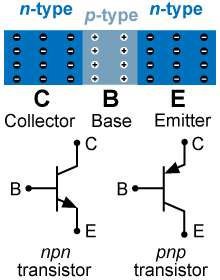
 A transistor is constructed from three semiconducting materials called the collector, base, and emitter. A transistor allows a very small current flowing in the base to control a much larger current from collector to emitter. A simple transistor has two p-n junctions back to back. The base terminal of an npn transistor is connected to the central p-type region. This layer is much thinner than the n-type layers on either side. A pnp transistor is the inverse, with an n-type semiconductor sandwiched between two layers of p-type. Transistors are the fundamental building blocks of electronic amplifiers, such as in your music player, and logic circuits in computers.
|

